


ЁЁ

|
|
|
|
|
|
|
|
|
|
|
|
|
|
|
|

|
ЁЁ |

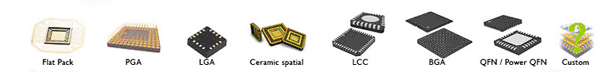
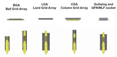
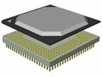
BGA/LGA/CGA/QFN/QFPИпЦЕВтЪдВхзљВњЦЗЗжЧђаЮГіНХ(SMT)КЭеыаЮГіНХМАНгДЅЪНШ§жжЩшМЦ.ЧђаЮГіНХЕФBGAВхзљЯЕЭГжївЊЪЪгУгкаОЦЌЕФВтЪдМАПЊЗЂЕШ.ИУВхзљЯЕЭГЕФЬиЕуЪЧВЛгУдкPCBАхЩЯПЊПз,BGAВхзљЕФКИНгЗНЗЈКЭBGAаОЦЌЕФКИНгЗНЗЈЭъШЋвЛбљ.ЭЌЪБШчЙћдкПЭЛЇЕФФПБъАхЩЯBGA
PadХдБпШчЙћвбОДцдквЛаЉЬљЦЌЦїМўЖјгАЯьЕНBGAВхзљЕФАВзА,ЮвУЧврЬсЙЉBGAВхзљЕФЩ§ИпЩшМЦвдБуТњзуПЭЛЇЕФЪЕМЪвЊЧѓ.ВПЗжBGAВхзљЛѕЦкИќЖЬжС2-3жмЁЃВЂПЩИљОнПЭЛЇЕФBGAЦїМўГіНХЃЌЖЈжЦКЯЪЪЕФBGAВхзљ(Available
for any chip size and grid pattern)ЁЃ
ЁЁ
ЁЁ
-
ЪЪКЯШЮКЮЗтзАжЎаОЦЌ.
-
здИаЯЕЪ§:аЁгк 2nH
-
жЇГжЦЕТЪЃКе§ГЃВЛДѓгк3Ghz,ЬиЪтЮЊ10Ghz,30Ghz
-
ЪЪКЯШЮКЮаОЦЌГпДчМАЧђеѓЗжВМ.
-
ГЌаЁГпДчЩшМЦ
-
ГіНХЗНЪНСщЛюЃКЧђаЭГіНХ, еыаЭГіНХ,НгДЅЪНЩшМЦУтКИНг.
-
ЕЏЛЩеыЩшМЦ,БмУтЖдЧђЬхдьГЩЩЫКІ.
-
ЭЌЪБМцШнBGA/LGAаОЦЌВтЪд.
-
жЇГжГЃЮТ,РЯЛЏ,ЕЭЦЕ,ИпЦЕВтЪд.
-
ЬсЙЉBGAВхзљЕФЩ§ИпЩшМЦвдБуТњзуПЭЛЇЕФЪЕМЪвЊЧѓ.
-
ПЩМгзАЩЂШШЦїЛђЗчЩШ.
 |
 |
 |
| Open Clameshell Type | ClamShell 'Injection mode' Type | Fast Lock |
 |
 |
 |
| Twist Lock | Clamshell | Solderless Compression Type |
 |
 |
 |
| Elastomer Socket | Quick Lock | QFN / MLF / MLP Socket |
 |
 |
 |
| QFP/PQFP/SOIC/SO etc | ClamShell 'Economy' Type | Sockets with SMT solderball adapters |
 |
 |
|
| BGA Adapters |
BGA Socket
Accessories & Spcecial Features BGAВтЪдВхзљХфМў |
|
 |
||
|
LGA to BGA converter plates For applications where a chip is tested with & without solderballs the LGA sockets can be delivered with a converter plate to allow socketing BGA chips with an LGA socket. |
||
ЁЁ
-
ШчКЮбЁдёЪЪКЯЕФВтЪдВхзљ(How
to choose a Socket)

-
E-tec Presentation - BGA
-
IC_BGA sockets - top view
dimensions
-
IC_BGA - BGA socket summary
-
IC_BGA - Recommended reflow
profile
-
IC_BGA - Socket Mounting
Recommendations
-
IC_BGA
adapter - solderball sockets
-
IC_BGA test report - 0.80 mm
pitch BGA sockets
-
IC_BGA test report - 1.00mm
pitch BGA sockets
-
IC_General specifications
-
E-tec / Sempac Alliance for
Prototyping sockets & chip packages
![]() ГЃгУBGAНХЮЛЭМ(BGA / LGA / CGA
/ QFP / CQFP Package)
ГЃгУBGAНХЮЛЭМ(BGA / LGA / CGA
/ QFP / CQFP Package)
ЁЁ
| Package | Socket Type | Part Number | Mechanical Drawing |
|---|---|---|---|
| BGA100,0.65mm Pitch | Clameshell,НгДЅЪН | BUC100-0690-10AA55L | BUC100-0690-10AA55L.pdf |
| CQFP48,0.5mm Pitch | Clameshell,ВхеыЪН | QFM048-1070-12AB95 | QFM048-1070-12AB95.pdf |
| CQFP100,0.5mm Pitch | Clameshell,ВхеыЪН | QFM100-0570-25AA95 | QFM100-0570-25AA95.pdf |
| CQFP100,0.5mm Pitch | Clameshell,НгДЅЪН | QFM100-0591-25AA95 | QFM100-0591-25AA55L.pdf |
| BGA100,0.65mm Pitch | Twist Lock,НгДЅЪН | BUP100-0690-10AL55L | BUP100-0690-10AL55L.pdf |
| BGA132,1.27mm Pitch | Fast Lock,еыаЭГіНХ | BPF132-1270-14AA95 | BPF132-1270-14AA95.pdf |
| BGA169 0.5mm Pitch | Fast Lock,НгДЅЪН | BPF169-0530-13AA95L | BPF169-0530-13AA95L.pdf |
| BGA256,1.0mm Pitch | Fast Lock,еыаЭГіНХ | BPF256-1070-20AA95 | BPF256-1070-20AA95.pdf |
| BGA256,0.8mm Pitch | Fast Lock,ElastomerРраЭ | EBF256-0891-16AA55L | EBF256-0891-16AA55L.pdf |
| BGA352,1.27mm Pitch | Fast Lock,еыаЭГіНХ | BPF352-1270-26AB95 | BPF352-1270-26AB95.pdf |
| BGA353,1.27mm Pitch | Fast Lock,НгДЅЪН | BPF353-1229-23AA95+L | BPF353-1229-23AA95+L.pdf |
| BGA360,1.27mm Pitch | Fast Lock,еыаЭГіНХ | BCF360-1270-19AA95 | BCF360-1270-19AA95.pdf |
| LGA360,1.27mm Pitch | Fast Lock,еыаЭГіНХ | LCF360-1270-19AA95 | LCF360-1270-19AA95.pdf |
| BGA361,1.27mm Pitch | Fast Lock,НгДЅЪН | BPF361-1290-19AA55L | BPF361-1290-19AA55L.pdf |
| BGA360,1.0mm Pitch | Twist Lock,НгДЅЪН,Щ§ИпЩшМЦ | BPW360-1029-22AC95+L | BPW360-1029-22AC95+L.pdf |
| BGA393,0.5mm Pitch | Twist Lock,НгДЅЪН | BUP393-0590-29AA55L | BUP393-0590-29AA55L.pdf |
| BGA393,0.5mm Pitch | Fast Lock,НгДЅЪН | BUB393-0590-29AL55L | BUB393-0590-29AL55L.pdf |
| LGA429,1.27mm Pitch | ЁЁFast Lock,еыаЭГіНХ | LPF429-1270-21AB95ЁЁ | LPF429-1270-21AB95.pdfЁЁ |
| BGA441,0.8mm Pitch | Twist Lock,ЧђаЭГіНХ | BUW441-0830-23AL95+L | BUW441-0830-23AL95+L.pdf |
| BGA480,1.27mm Pitch | Twist Lock,НгДЅЪН | BPW480-1290-29AL55L | BPW480-1290-29AL55L.pdf |
| BGA480,1.27mm Pitch | Clameshell,НгДЅЪН | BCC480-1290-29AA55L | BCC480-1290-29AA55L.pdf |
| BGA484,1.27mm Pitch | Fast Lock,НгДЅЪН | BCF484-1290-22AAA55L | BCF484-1290-22AAA55L.pdf |
| BGA532,0.8mm Pitch | Clameshell,ЧђаЭГіНХ | BPC532-0830-26AA95+L | BPC532-0830-26AA95+L.pdf |
| CGA560,1.27mm Pitch | Fast Lock,ЧђаЭГіНХЁЁ | CCF560-1230-33AB95+LЁЁ | CCF560-1230-33AB95+L.pdfЁЁ |
| BGA560,1.27mm Pitch | Fast Lock,ЧђаЭГіНХ | BPF560-1230-33AB95+L | BPF560-1230-33AB95+L.pdf |
| BGA576,1.0mm Pitch | E-Clameshell,НгДЅЪН | BPE0576-10-09542-24AAA-L | BPE0576-10-09542-24AAA-L.pdf |
| BGA576,1.0mm Pitch | Fast Lock,НгДЅЪН | BPF0576-10-09542-24AAA-L | BPF0576-10-09542-24AAA-L.pdf |
| BGA676,1.0mm Pitch | Clameshell,ЧђаЭГіНХ | BPC676-1030-26AA95+L | BPC676-1030-26AA95+L.pdf |
| BGA697,1.0mm Pitch | Fast Lock,ЧђаЭГіНХ | BPF697-0830-29AA95+L | BPF697-0830-29AA95+L.pdf |
| BGA697,1.0mm Pitch | Fast Lock,ЧђаЭГіНХ,Щ§ИпЩшМЦ | BPF697-0829-29AA95+L | BPF697-0829-29AA95+L.pdf |
| CGA717,1.27mm Pitch | Twist Lock,ЧђаЭГіНХ | CCW717-1230-27AA95+L | CCW717-1230-27AA95+L.pdf |
| CGA717,1.27mm Pitch | Twist Lock,еыаЭГіНХ | CCW717-1270-27AA95 | CCW717-1270-27AA95.pdf |
| CGA717,1.27mm Pitch | FastLock,НгДЅЪН | CPF717-1290-27AA55L | CPF717-1290-27AA55L.pdf |
| CGA1144,1.0mm Pitch | FastLock,еыаЭГіНХ | CPF1144-1070-34AA95 | CPF1144-1070-34AA95.pdf |
| CGA1509,1.0mm Pitch | FastLock,еыаЭГіНХ | CPF1509-1070-39AA95 | CPF1509-1070-39AA95.pdf |
| BGA896,1.0mm Pitch | FastLock,ВхеыГіНХ,ДјЩЂШШЦЌ | BPF896-1070-30AA95H | BPF896-1070-30AA95H.pdf |
| BGA896,1.0mm Pitch | Clameshell,ВхеыГіНХ,ДјЩЂШШЦї | BPE896-1070-30AA95H | BPE896-1070-30AA95H.pdf |
| BGA1121,1.0mm Pitch | Fast Lock,еыаЭГіНХ,Щ§ИпЩшМЦ | BUF1121-1029-39AA95H+L | BUF1121-1029-39AA95H+L.pdf |
| BGA1121,1.0mm Pitch | Clameshell,ВхеыГіНХ | LPE1121-1070-39AB95C | LPE1121-1070-39AB95C.pdf |
| BGA1517,1.0mm Pitch | FastLock,ЧђаЭГіНХ | BPF1517-1030-39AA95+L | BPF1517-1030-39AA95+L.pdf |
ЁЁ
|
ЩюлкЪаСтУРЕчзггаЯоЙЋЫО АцШЈЫљга ЕчзггЪМў:sales@lingmei.com.cn гЪеўБрТыЃК518033 СЊЯЕЕчЛАЃК+86 755 82915895 82915035 82915136 ДЋецЃК+86 755 82916505 |